Components found burnt out when assembling finished goods in the system manufacturers, and the IC design house claims EOS is to blame.
As an IC designer, how do you quickly identify the location of burns and change circuits?
Static exists everywhere. Components tend to burn out due to electrical over stress (EOS) under current or voltage overload.
Finished goods manufacturers are pressed to deliver products as scheduled while assemblers are squeezing IC design houses to come up with solutions. Being an IC designer, what should you do to identify burnt areas in order to proceed with circuit design modification? The iST Tech Classroom presents some typical cases to help you pinpoint component EOS abnormal hot spots in 3 simple steps.
Step 1: Localization
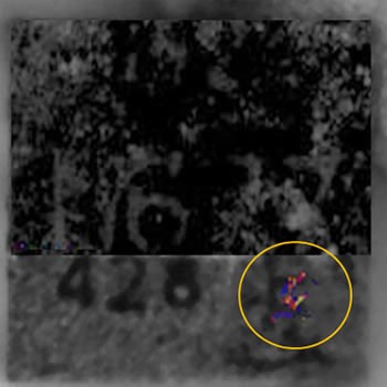
Detect packaging defect by phase differences of thermal radiation at the failure point without damaging powered devices to quickly position the failure point (getting its XYZ coordinates).
Step 2: Identify delamination
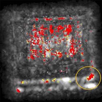
Components suffering EOS tend to result in IC surface and packaging layer damaged due to high temperature which, in turn, leads to delamination at the EOS point. A scan with a non-destructive SAT (Scanning Acoustic Tomography) ultrasound may identify the position of packaging layer delamination, which is in the same location pinpointed by the thermal EMMI.
Step 3: Take out the die
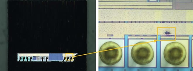
By taking out dies at the failure position detected by SAT and the thermal EMMI and visually checking these dies with an OM digital microscope, it’s easy to identify EOS burnt areas that fall in between the die surface and black compound.
iST
Integrated Service Technology
Taiwan•China•USA•Japan
Your Faithful Lab Partner
www.istgroup.com
Website handcrafted by Emily Lieberman, Digital Girl
Copyrights Reserved to Icleviathan Ltd. ©